
-
Capability
-
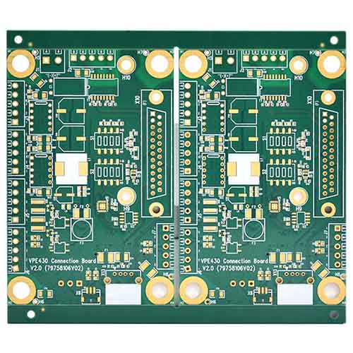
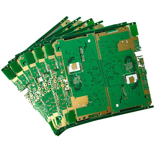
Standard PCB Capabilities
| ltem | Capability |
|---|---|
| Layer Count | 1-40layers |
| Base Material | KB、Shengyi、ShengyiSF305、FR408、FR408HR、IS410、FR406、GETEK、370HR、IT180A、Rogers4350、Rogers4000、PTFE Laminates(Rogers series、Taconic series、Arlon series、Nelco series)、Rogers/Taconic/Arlon/Nelco laminate with FR-4 material (including partial Ro4350B hybrid laminating with FR-4) |
| Board Type | Backplane、HDI、High multi-layer blind&buried PCB、Embedded Capacitance、Embedded resistance board 、Heavy copper power PCB、Backdrill, PCB Gold Finger |
| Board Thickness | 0.2-5.0mm |
| Copper Thickness | Min. 1/2 OZ, Max. 10 OZ |
| PTH Wall | 25um(1mil) |
| Maximum Board Size | 1100*500mm(43”*19”) |
| Min laser drilling size | 4mil |
| Min. Spacing/Tracing | 2.7mil/2.7mil |
| Solder Mask | Green, Black, Blue, Red, White, Yellow, Purple matte/glossy |
| Surface Treatment | Flash gold(electroplated gold)、ENIG、Hard gold、Flash gold、HASL Lead-free 、OSP、ENEPIG、Soft gold、Immersion silver、Immersion Tin、ENIG+OSP, ENIG+Gold finger, Flash gold(electroplated gold)+Gold finger(50u”), Immersion silver+Gold finger, Immersion Tin+Gold finger |
| Min. Annular Ring | 3mil |
| Aspect ratio | 10:1(HASL Lead-free 、HASL Lead、ENIG、Immersion Tin、Immersion silver、ENEPIG);8:1(OSP) |
| Impedance control | ±5ohm(<50ohm), ±10%(≥50ohm) |
| Other Techniques | Blind/Buried Via, Gold Fingers, Press Fit, Via in Pad, Electrical Test |
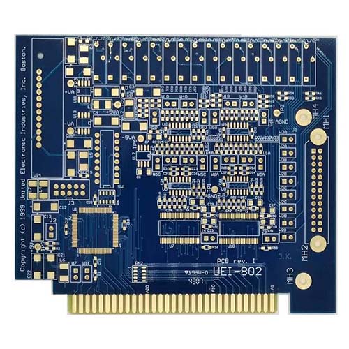
Most electronic appliances require complex electronic circuits.
This is why designers have to arrange tiny electronic components on an electronic board.
It includes a plastic board with copper tracks on one side and many holes for fixing components.
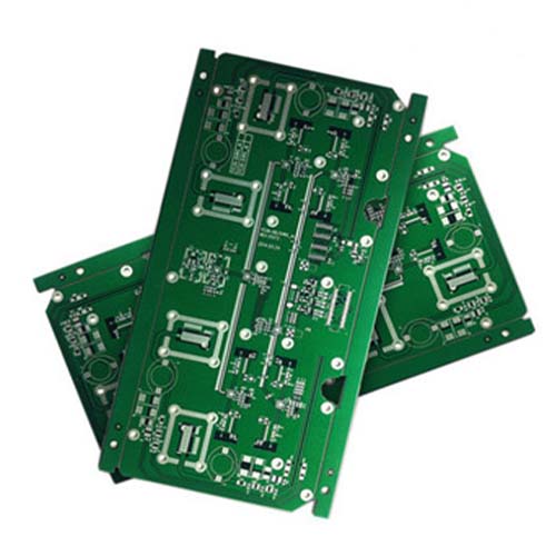
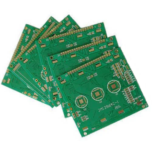
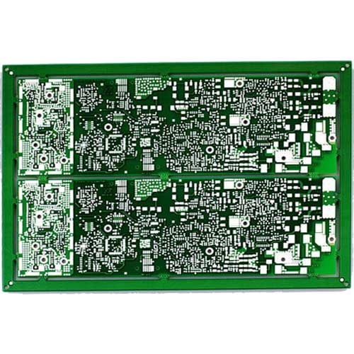
When a circuit board layout is printed on a plastic board, it is called a standard PCB.
The PCB is the element behind how many electronic products work – from home appliances to toys.
Its importance is essential for a variety of applications and can be mass-produced after design.
To make assembly of electronic components it is necessary to have advanced skills, in order to satisfy an increasingly vast market.
What is Standard PCB Thickness
Many PCB manufacturers may say that the standard PCB thickness is 1.60mm, or approximately 0.062 in.
This is true to an extent. Apparently, this was the size that bakelite sheets were manufactured in during the earlier days of board fabrication and the size has stuck.
Therefore, we can refer to this as the historical standard PCB thickness.
Today, boards are made to be larger and smaller than this standard, but the standard probably remains the most common thickness for designs.
Today, it is more accurate to say there is a range of common or standard PCB thicknesses.
These include 0.031in (0.80mm ), 0.062in (1.60mm) and 0.093in (2.40mm). Depending on your choice for PCB fabrication and assembly services, you may be able to have boards made with other thicknesses.
When determining the PCB thickness, there a number of design and manufacturing factors to consider, as listed below.
Design Factors that Impact PCB Thickness
- Copper thickness
- Board materials
- Number of PCB layers
- Signal types
- Types of vias
- Operating environment
Manufacturing Factors Affecting Standard PCB Thickness
- Drill hole equipment
- Copper thickness
- Layer count
- Depanelization method
Based on Application Needs
Depending on the application’s needs, different types of PCB printed circuits can be used.
It is possible to indicate those that are the most widespread and sought after, namely those with single and double-sided, without forgetting, however, that multilayer and with aluminum support.
The standard PCB circuits differ in relation to the working frequencies, the current power, and the specific uses in the various reference sectors.
This makes it clear how different the approach for their creation must also be – from time to time.
In general, it is correct to say that the simplest and cheapest models are the monolayer ones, that is single-sided.
Those with double faces are already more complex and able to solve different problems. While as regards the multilayer circuits, they are composed of different layers of conductive material: the realizations that allow obtaining are decidedly more complex.
The different phases of design and construction are carried out and monitored with the aid of PCs and dedicated equipment: it is necessary to guarantee compliance with the indications given by the customer.
Moreover, the products must pass strict controls to obtain certificates of conformity.
Frequently Asked Questions
1. What is the difference between OEM PCB and standard PCB?
2. What does the design process for Wenshu PCB involve?
3. How can product reliability and quality be ensured in Wenshu PCB design?
4. How can confidentiality be maintained in the manufacturing process of Wenshu PCBs?
Why Choose Us

Responsive Service
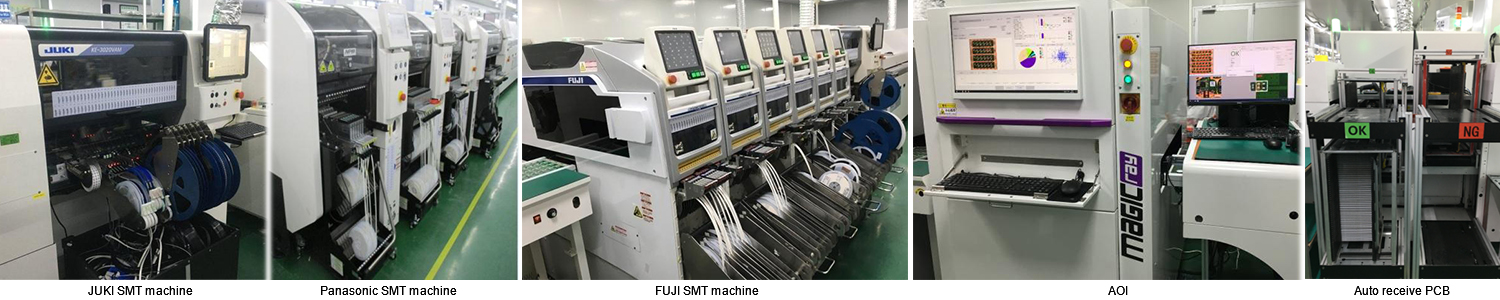
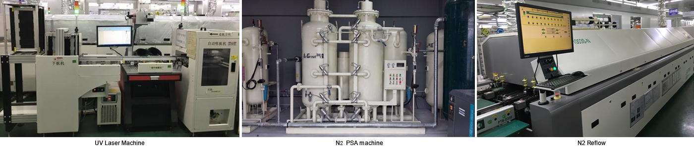
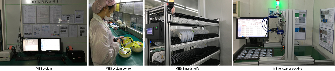
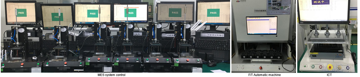
Using state-of-the-art automated SMT and through-hole lead free wave soldering, we're committed to responsive service from first contact to delivery..

Rich Experience
With 18 years of experience in providing box build services, we have all the expertise needed to ensure our products are manufactured to the highest standards.

Turnkey Box Build Assembly
With NEWHONEST box build services, you will receive complete support for the entire mechanical assembly process, ranging from component sourcing, design, manufacturing, testing, and repair.

High-Quality Guaranteed
Our certifications guarantee the quality of our products and services, we are ISO 9001, ISO13485, IPC-A-610, RoHS & Lead-Free process certified, registered, and REACH compliant.
