
-
Capability
-
High Frequency PCB Capabilities
| ltem | Capability |
|---|---|
| Material | FR-4 Standard Tg 140°C, FR4-High Tg 170°C |
| Min. Track/Spacing | For External layers: 4oz Cu 10mil/13mil, 5oz Cu 12mil/15mil, 6oz Cu 15mil/15mil For Internal layers: 4oz Cu 8mil/8mil, 5oz Cu 10mil/10mil, 6oz Cu 12mil/12mil |
| Min. Hole Size | 0.15 ~ 0.3mm |
| Max Outer Layer Copper Weight (Finished) | 12oz |
| Max Inner Layer Copper Weight | 12oz |
| Board Thickness | 0.6-6mm |
| Surface Finishing | HASL lead-free, Immersion gold, OSP, Hard Gold, Immersion Silver, Enepig |
| Solder Mask | Green, Red, Yellow, Blue, White, Black, Purple, Matte Black, Matte green |
| Silkscreen | White, Black |
| Via Process | Tenting Vias, Plugged Vias, Vias not covered |
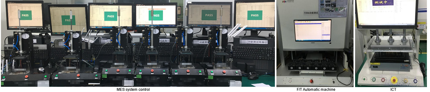
| Testing | Fly Probe Testing (Free) and A.O.I. testing |
| Build time | 5-15 days |
| Lead time | 2-3 days |
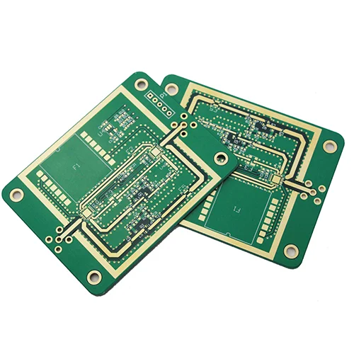
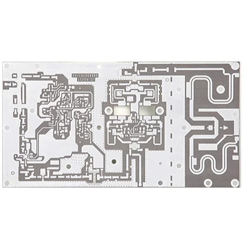
Introducing our high-Frequency PCB, the pinnacle of excellence in the realm of RF and microwave applications. Designed to meet the demanding requirements of high-frequency signals, our high-frequency PCBs offer exceptional performance, reliability, and signal integrity.
Our high-frequency PCBs are meticulously engineered using specialized materials and advanced manufacturing techniques. These PCBs are specifically tailored to operate in the microwave and RF frequency range.
Moreover, this makes them ideal for applications such as wireless communications, satellite systems, radar systems, and high-speed data transmission.
Advantages of High-Frequency PCB:
- Excellent Signal Integrity: High-frequency PCBs are designed to maintain signal integrity and minimize signal loss at high frequencies. These PCBs utilize low-loss materials with controlled dielectric constants. Moreover, it ensures a superior impedance control, reduced insertion loss, and improved return loss.
- Wide Frequency Range: Our high-frequency PCBs are capable of operating in a wide frequency range, from a few megahertz (MHz) to several gigahertz (GHz). This versatility makes them suitable for a variety of applications, including wireless communication systems, microwave devices, and high-speed digital circuits.
- Low Transmission Loss: High-frequency PCBs are built using materials with low dissipation factors and low dielectric losses. This results in minimal transmission loss, allowing for efficient signal transmission and reception, especially in high-speed and high-frequency applications.
- Impedance Control: Maintaining impedance control is crucial for high-frequency signals. Our high-frequency PCBs are engineered to provide precise impedance matching, ensuring maximum power transfer and minimizing signal reflections. This also leads to improved system performance and reduced signal distortions.
- High Thermal Stability: High-frequency PCBs are designed to withstand the challenges of thermal management in high-power applications. They employ thermally conductive materials and efficient heat dissipation techniques. It also ensures stable performance even under elevated temperature conditions.
Frequently Asked Questions
1. What is the difference between OEM PCB and standard PCB?
2. What does the design process for Wenshu PCB involve?
3. How can product reliability and quality be ensured in Wenshu PCB design?
4. How can confidentiality be maintained in the manufacturing process of Wenshu PCBs?
Why Choose Us

Responsive Service
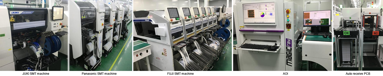
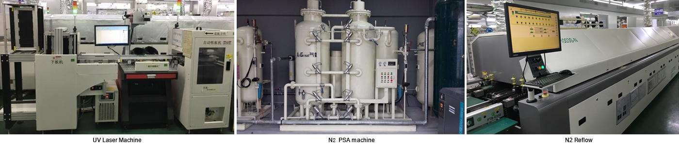
Using state-of-the-art automated SMT and through-hole lead free wave soldering, we're committed to responsive service from first contact to delivery..

Rich Experience
With 18 years of experience in providing box build services, we have all the expertise needed to ensure our products are manufactured to the highest standards.

Turnkey Box Build Assembly
With NEWHONEST box build services, you will receive complete support for the entire mechanical assembly process, ranging from component sourcing, design, manufacturing, testing, and repair.

High-Quality Guaranteed
Our certifications guarantee the quality of our products and services, we are ISO 9001, ISO13485, IPC-A-610, RoHS & Lead-Free process certified, registered, and REACH compliant.
