
-
Capability
-
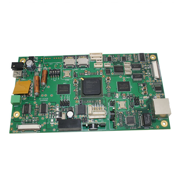
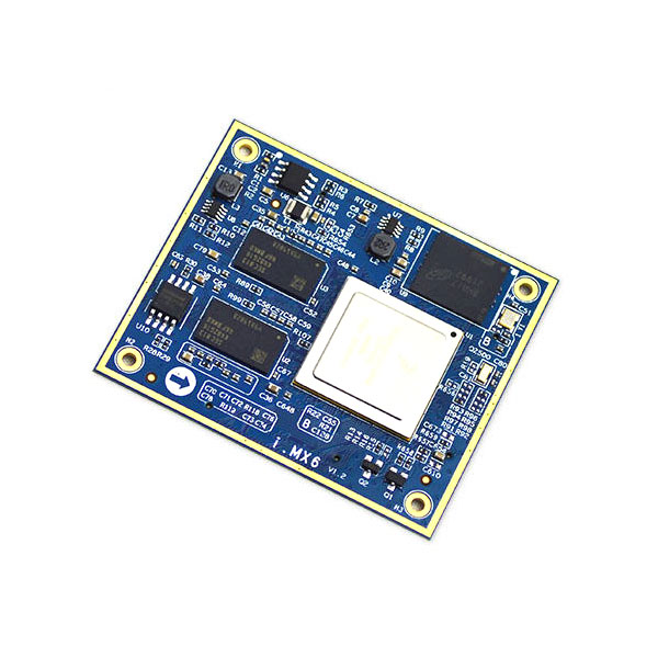
BGA Assembly Capabilities
| ltem | Capability |
|---|---|
| Order Quantity | ≥1PC |
| Quality Grade | IPC-A-610 |
| Lead Time | 24 hours expedited service can be offered. 3- 4 days normally for PCBA prototype orders. We will give you an accurate lead time when we quote for you. |
| Size | 50*50mm~510*460mm |
| Board Type | Rigid PCB, Flexible PCB, metal core PCB |
| Min Package | 01005 (0.4mm*0.2mm) |
| Max Package | No limit |
| Mounting Accuracy | ±0.035mm(±0.025mm) Cpk≥1.0 (3σ) |
| Surface Finish | Lead/Lead-free HASL, Immersion gold, OPS, etc. |
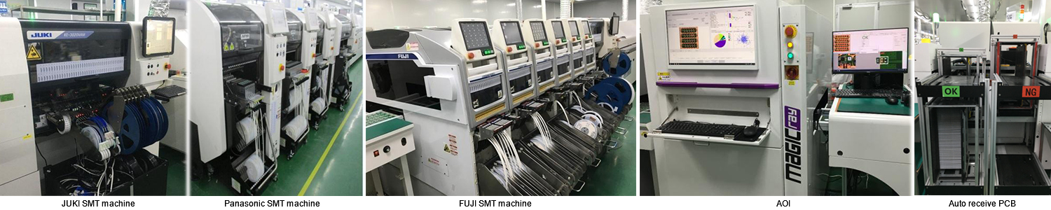
| Assembly Types | Surface mount (SMT), Through-hole (DIP), Mixed Technology (SMT & Thru-hole) |
| Component Sourcing | Turnkey (All components sourced by Wenshu), Partial turnkey, Kitted/Consigned |
| BGA Package | BGA Dia. 0.14mm, BGA 0.2mm pitch |
| Cable Assembly | We supply custom cables, cable assemblies, wiring looms/harnesses and power leads for various industries including automotive, security, mining, medical and entertainment. |
| Stencil | Stencil with or without frame (offered free by Wenshu) |
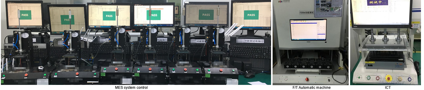
| Quality Inspection | Visual inspection; AOI checking; BGA placement – X-RAY checking |
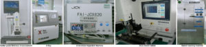
To achieve the highest quality standards for BGA assembly, we use a variety of inspection methods throughout the process including optical inspection, mechanical inspection, and X-ray inspection. Among them, the inspection of BGA solder joints must use X-rays. X-rays can pass through the components to inspect the solder joints below them, so as to check the solder joint position, solder joint radius, and solder joint thickness.
Efficient Use of Space – BGA PCB layout allows us to efficiently use the available space, so we can mount more components and manufacture lighter devices.
Better Thermal Performance – For BGA, the heat generated by the components is transferred directly through the ball. In addition, the large contact area improves heat dissipation, which prevents overheating of components and ensures long life.
Higher Electrical Conductivity – The path between the die and the circuit board is short, which results in better electrical conductivity. Moreover, there is no through-hole on the board, the whole circuit board is covered with solder balls and other components, so vacant spaces are reduced.
Easy to Assemble And Manage – Compared to other PCB assembly techniques, BGA is easier to assemble and manage as the solder balls are used directly to solder the package to the board.
Less Damage to Leads – We use solid solder balls for manufacturing BGA leads. Hence, there is a lesser risk that they will get damaged during the operation.
Frequently Asked Questions
1. What is the difference between OEM PCB and standard PCB?
2. What does the design process for Wenshu PCB involve?
3. How can product reliability and quality be ensured in Wenshu PCB design?
4. How can confidentiality be maintained in the manufacturing process of Wenshu PCBs?
Why Choose Us

Responsive Service
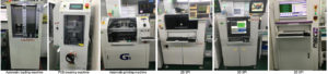
Using state-of-the-art automated SMT and through-hole lead free wave soldering, we're committed to responsive service from first contact to delivery..

Rich Experience
With 18 years of experience in providing box build services, we have all the expertise needed to ensure our products are manufactured to the highest standards.

Turnkey Box Build Assembly
With NEWHONEST box build services, you will receive complete support for the entire mechanical assembly process, ranging from component sourcing, design, manufacturing, testing, and repair.

High-Quality Guaranteed
Our certifications guarantee the quality of our products and services, we are ISO 9001, ISO13485, IPC-A-610, RoHS & Lead-Free process certified, registered, and REACH compliant.
