
-
Capability
-
HDI PCB Capabilities
| ltem | Capability |
|---|---|
| Material | FR-4 Standard Tg 140°C, FR4-High Tg 170°C |
| Min. Track/Spacing | For External layers: 4oz Cu 10mil/13mil, 5oz Cu 12mil/15mil, 6oz Cu 15mil/15mil For Internal layers: 4oz Cu 8mil/8mil, 5oz Cu 10mil/10mil, 6oz Cu 12mil/12mil |
| Min. Hole Size | 0.15 ~ 0.3mm |
| Max Outer Layer Copper Weight (Finished) | 12oz |
| Max Inner Layer Copper Weight | 12oz |
| Board Thickness | 0.6-6mm |
| Surface Finishing | HASL lead-free, Immersion gold, OSP, Hard Gold, Immersion Silver, Enepig |
| Solder Mask | Green, Red, Yellow, Blue, White, Black, Purple, Matte Black, Matte green |
| Silkscreen | White, Black |
| Via Process | Tenting Vias, Plugged Vias, Vias not covered |
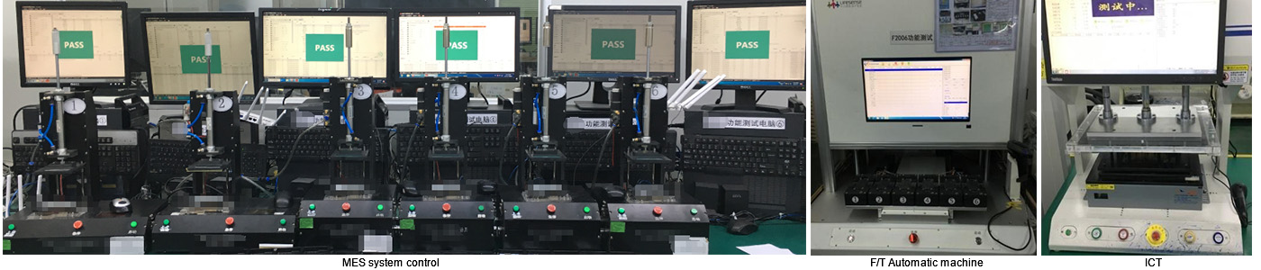
| Testing | Fly Probe Testing (Free) and A.O.I. testing |
| Build time | 5-15 days |
| Lead time | 2-3 days |
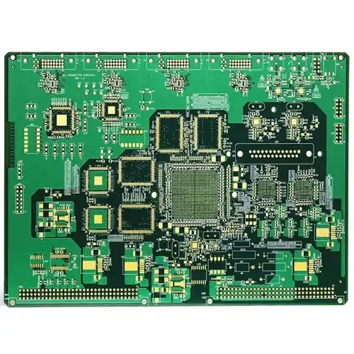
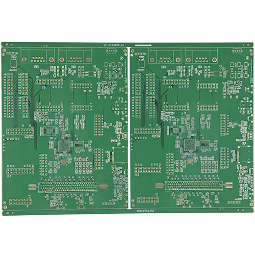
HDI PCB fabrication is rapidly becoming the ultimate solution for smaller, more efficient, and more durable PCBs. High-Density Interconnect (HDI) is a high-performance design that is characterized by its high density of components and routing Interconnections that use micro vias, blind and buried via or micro via techniques, and built-up Print Circuit Boards (PCBs) laminations.
As HDI PCBs specialist, Wenshu has extensive experience in manufacturing HDI PCBs for customers in different industries such as medical, automotive, and electronics. We have the ability to handle all HDI PCBs projects with unmatched accuracy and high quality within your budget.
Frequently Asked Questions
1. What is the difference between OEM PCB and standard PCB?
2. What does the design process for Wenshu PCB involve?
3. How can product reliability and quality be ensured in Wenshu PCB design?
4. How can confidentiality be maintained in the manufacturing process of Wenshu PCBs?
Why Choose Us

Responsive Service
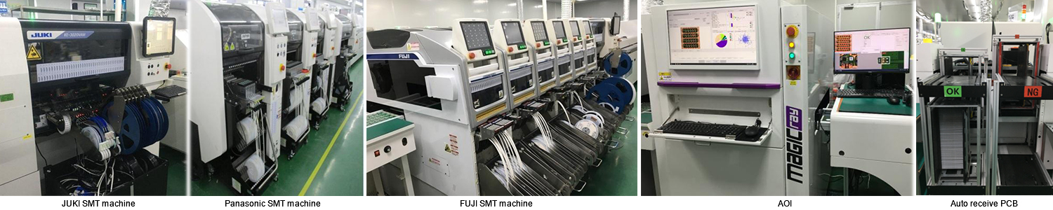
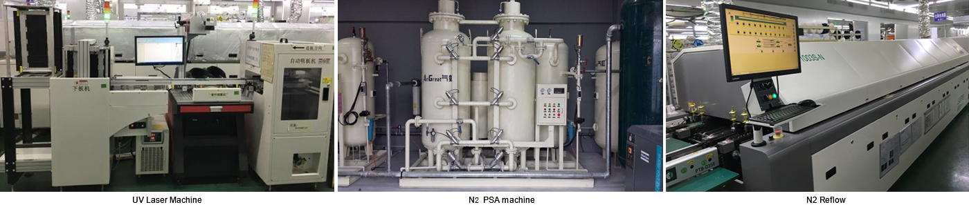
Using state-of-the-art automated SMT and through-hole lead free wave soldering, we're committed to responsive service from first contact to delivery..

Rich Experience
With 18 years of experience in providing box build services, we have all the expertise needed to ensure our products are manufactured to the highest standards.

Turnkey Box Build Assembly
With NEWHONEST box build services, you will receive complete support for the entire mechanical assembly process, ranging from component sourcing, design, manufacturing, testing, and repair.

High-Quality Guaranteed
Our certifications guarantee the quality of our products and services, we are ISO 9001, ISO13485, IPC-A-610, RoHS & Lead-Free process certified, registered, and REACH compliant.
