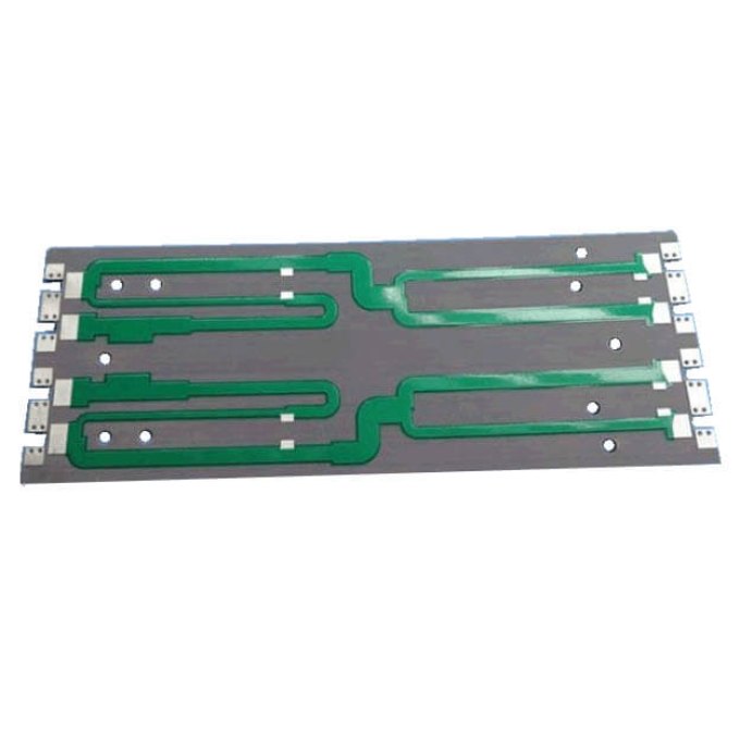
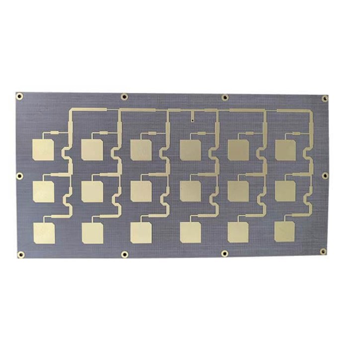
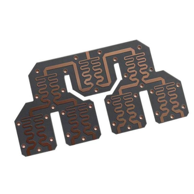
High Speed PCB
Wenshu is a professional high speed PCB manufacturer in China. As 5G era is coming, high speed PCBs need more and more in different applications.
| Layer Count | 1-40layers |
| Board Thickness | 0.2-5.0mm |
| Copper Thickness | Min. 1/2 OZ, Max. 10 OZ |
| PTH Wall | 25um(1mil) |
| Maximum Board Size | 1100*500mm(43”*19”) |
| Min laser drilling size | 4mil |

Prototype to Full Turn-Key Assembly

Through-Hole Lead-Free Wave Soldering

Best Price, Genuine Components

Quality Accreditation ISO9001
-
Description
-
Specification
Wenshu is a professional high speed PCB manufacturer in China. As 5G era is coming, high speed PCBs need more and more in different applications.
- Over 12 years high speed PCB manufacturing experience
- No minimum order quantity for high speed PCB order
- Complete PCB material in stock like Taconic, Rogers, Arlon
- 100% E-test and AOI inspection
- 24h quick turn service for your prototype of high speed PCB
In short, high-speed PCB design refers to any design where signal integrity begins to be affected by the physical characteristics of the circuit board, such as layout, packaging, layer stacking, interconnection, etc. To delay, attenuation, crosstalk, reflection or emission, etc.
As a reliable high speed PCB supplier, Wenshu has one engineering team over 20 years design experience. We have served over 1000+ customers all around the world.
Wenshu has many selections of high speed PCB design software, for example Altium Designer, Cadence Or CAD, Legacy PCAD, Eagle (Altium Conversion). Please tell us which software you need us to use in your project.
The reason why the high speed PCB design is so unique is the level of attention paid to these issues. You may be accustomed to designing simple circuit boards, where most of your time is spent on component placement and routing.
But for high speed PCB design, it is more important to accurately consider the placement of the trace, the width of the trace, the distance from other signals, and the type of connected components.
| ltem | Capability |
|---|---|
| Layer Count | 1-40layers |
| Base Material | KB、Shengyi、ShengyiSF305、FR408、FR408HR、IS410、FR406、GETEK、370HR、IT180A、Rogers4350、Rogers4000、PTFE Laminates(Rogers series、Taconic series、Arlon series、Nelco series)、Rogers/Taconic/Arlon/Nelco laminate with FR-4 material (including partial Ro4350B hybrid laminating with FR-4) |
| Board Type | Backplane、HDI、High multi-layer blind&buried PCB、Embedded Capacitance、Embedded resistance board 、Heavy copper power PCB、Backdrill, PCB Gold Finger |
| Board Thickness | 0.2-5.0mm |
| Copper Thickness | Min. 1/2 OZ, Max. 10 OZ |
| PTH Wall | 25um(1mil) |
| Maximum Board Size | 1100*500mm(43”*19”) |
| Min laser drilling size | 4mil |
| Min.spacing/Tracing | 2.7mil/2.7mil |
| Solder Mask | Green, Black, Blue, Red, White, Yellow, Purple matte/glossy |
| Surface Treatment | Flash gold(electroplated gold)、ENIG、Hard gold、Flash gold、HASL Lead-free 、OSP、ENEPIG、Soft gold、Immersion silver、Immersion Tin、ENIG+OSP, ENIG+Gold finger, Flash gold(electroplated gold)+Gold finger(50u”), Immersion silver+Gold finger, Immersion Tin+Gold finger |
| Min. Annular Ring | 3mil |
| Aspect ratio | 10:1(HASL Lead-free 、HASL Lead、ENIG、Immersion Tin、Immersion silver、ENEPIG);8:1(OSP) |
| Impedance control | ±5ohm(<50ohm), ±10%(≥50ohm) |
| Other Techniques | Blind/Buried Via, Gold Fingers, Press Fit, Via in Pad, Electrical Test |