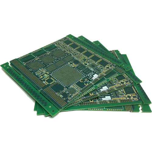
14-Layer PCB Circuit Board
A 14-layer PCB circuit board stackup can be referred to as a multi-layer printed circuit board device, and it must be used whenever you need 8 signal layers. In addition to that, when you need a special shield made of net, a 14-layer pcb stackup will be required.
| Layers | 14L |
| Panel size | 120*95mm/1 |
| Plate Thickness | 2.4mm |
| Minimum through hole | 0.20mm |
| Minimum BGA | 0.25mm |
| Line width line spacing | 3/3.2mil |

Prototype to Full Turn-Key Assembly

Through-Hole Lead-Free Wave Soldering

Best Price, Genuine Components

Quality Accreditation ISO9001
-
Description
-
Specification
The 14-layer PCB circuit board stackup has a variety of uses. It is useful in applications such as satellite dishes, preamplifiers, memory modules, SAN storage, AC drives, etc.
A 14-layer PCB circuit board stackup can be referred to as a multi-layer printed circuit board device, and it must be used whenever you need 8 signal layers. In addition to that, when you need a special shield made of net, a 14-layer pcb stackup will be required.
14-layer PCB circuit board stack-up application
Today, many industries use 14-layer pcb stack-ups for different applications. They have different uses and we can also say that it is useful in all areas of the PCB industry.
Here are the areas where the 14-layer PCB stackup is applicable.
Industry
14-layer PCB stackup is now a well-known name in different industrial applications. It is useful in control systems and industrial computers. They are also suitable for industrial and manufacturing applications where they are useful in running machinery. This is because of the small size, functionality and durability of the 14-layer PCB stackup.
Electronic product
Microwave ovens and smartphones are well-known electronic gadgets that people use regularly. All of these products use printed circuit boards, but more products now prefer to use a 14-layer PCB stackup instead of the usual single-layer PCB.
Car
The headlight switch, onboard computer, GPS, engine sensor use a 14-layer PCB stackup. Furthermore, electric vehicles utilize this stack-up in different applications.
Medical equipment
A large number of electronic devices in the healthcare sector use a 14-layer PCB stackup. These devices include equipment for X-rays, CAT scans, medical tests, and heart monitors.
Telecommunications
Devices used in telecommunications use 14-layer PCB stack-ups in many of their general-purpose applications. Some of these include GPS, signaling, satellite applications, and more. Outdoor towers or mobile equipment typically utilize telecommunications applications that use a 14-layer PCB stackup.
14-layer PCB stackup benefits
From a design standpoint, the 14-layer PCB stackup offers several benefits. These benefits include:
High quality
There is a lot of work and planning to do before creating a 14-layer PCB stackup. That’s why 14-layer PCB stack-up has better quality compared to other PCB stack-ups. They are also more reliable.
Small size
This PCB stack-up is smaller compared to other stack-ups with similar functionality. This is due to its layered design. Additionally, the smaller and more compact size of the 14-layer PCB stackup gives it an advantage in modern technology.
Power increase
A 14-layer PCB stack-up integrates multiple layers on one printed circuit board. This is one of the reasons why they offer blazing fast speeds.
More durable
With a 14-layer PCB stackup, you’ll easily handle extreme pressure and heat and withstand their weight. Here you can connect the layers with prepregs and other useful materials. In this case, the stack provides sufficient insulation. These features make the 14-layer PCB stack-up more durable.
Flexibility
The 14-layer PCB stack-up utilizes flexible construction techniques. This is what makes your printed circuit board more flexible. You need the flexibility to bend and bend in situations where slight bends and bends are possible in semi-regular situations.
| Feature | Capability |
|---|---|
| Material | FR-4 Standard Tg 140°C, FR4-High Tg 170°C |
| Min. Track/Spacing | For External layers: 4oz Cu 10mil/13mil, 5oz Cu 12mil/15mil, 6oz Cu 15mil/15mil For Internal layers: 4oz Cu 8mil/8mil, 5oz Cu 10mil/10mil, 6oz Cu 12mil/12mil |
| Min. Hole Size | 0.15 ~ 0.3mm |
| Max Outer Layer Copper Weight (Finished) | 12oz |
| Max Inner Layer Copper Weight | 12oz |
| Board Thickness | 0.6-6mm |
| Surface Finishing | HASL lead-free, Immersion gold, OSP, Hard Gold, Immersion Silver, Enepig |
| Solder Mask | Green, Red, Yellow, Blue, White, Black, Purple, Matte Black, Matte green |
| Silkscreen | White, Black |
| Via Process | Tenting Vias, Plugged Vias, Vias not covered |
| Testing | Fly Probe Testing (Free) and A.O.I. testing |
| Build time | 5-15 days |
| Lead time | 2-3 days |