Medical Device PCB
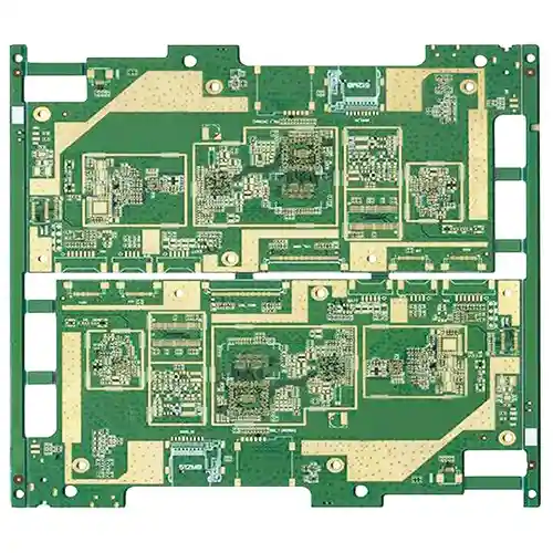
The Medical device PCB Printed Circuit Board (PCB) business has expanded its irresistible beneficial influence due to the continuous growth of the tech world and its use in various fields. In recent years, its impact on the world of electronics has exceeded all forecasts, including IoT devices, smartphones, computers, artificial intelligence, and more.
| Laminate | 8L |
| Dielectric constant | 4.2 |
| Plate Thickness | 1.6MM |
| Minimum Aperture: | 0.2mm |
| Minimum line width | 0.1MM |
| Minimum line spacing | 0.1MM |

Prototype to Full Turn-Key Assembly

Through-Hole Lead-Free Wave Soldering

Best Price, Genuine Components

Quality Accreditation ISO9001
-
Description
-
Specification
The Medical device PCB Printed Circuit Board (PCB) business has expanded its irresistible beneficial influence due to the continuous growth of the tech world and its use in various fields. In recent years, its impact on the world of electronics has exceeded all forecasts, including IoT devices, smartphones, computers, artificial intelligence, and more.
Now, PCBs are transforming medical devices and bridging the gap between patients and physicians in the medical technology business.
PCB, enabling the development of these convenient medical devices. Advances in healthcare technology are helping to solve several key challenges in the medical field, such as establishing accurate diagnoses and tracking patient health.
The medical electronics industry is growing rapidly and does not seem to be slowing down, which shows the influence of PCBs in the medical field. The global medical electronics market is expected to reach $4.4 billion by 2022. With the advancement of technology, PCBs are becoming more and more important in the medical field. Due to their digital nature, most medical devices and gadgets today require PCBs to work correctly and efficiently.
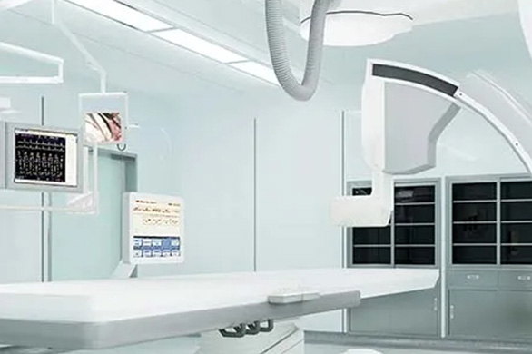
PCBs are required to operate medical devices such as defibrillators, electrical muscle stimulation devices, MRI, medical imaging systems, CT scans, and ultrasound equipment.
Medical Device PCB Technology and Its Types
Extra care must be taken to ensure reliability when producing medical PCBs. This is especially true for those used in implants. First, they must be hygienic. They also have to be more compact than usual. Therefore, HDI (High-Density Interconnect) PCBs are used in most medical devices.
The following are the techniques used in medical PCB assembly:
HDI / via-in-pad technology
The design of inserting vias inside copper pads is called via-in-pad and is often used to save space on the PCB. With in-pad technology, the PCB can provide up to 50% more space for component placement. The widespread use of vias in pads by PCB engineers is in pursuit of more acceptable pitch for devices and smaller electronics.
Surface Mount Technology
Surface Mount Technology, or SMT, is now used in nearly all commercially manufactured devices because it offers huge advantages in the PCB manufacturing process and, due to the smaller size of SMT components, allows more electronic devices to be packaged into smaller in a small space. In addition to being compact, surface mount technology (SMT) enables automated soldering and PCB assembly, improving reliability and saving money.
PCB fine lines and spaces
Next-generation portable electronic devices will rely heavily on high-density interconnect (HDI) PCB technology, including tiny lines and spaces (2 mils and below). This technology has several advantages over conventional techniques, including reduced board size, enhanced wiring, and cheaper manufacturing costs.
Application of Medical PCB in Healthcare Industry
Printed circuit boards and electronics play a vital role in the medical industry. Furthermore, with the advancement of technology, PCBs in the healthcare industry are rapidly expanding, opening up new possibilities.
PCBs are commonly used in the following applications:
Scanning equipment: CT scanners, X-ray screens, and ultrasound scans all rely on electronic components to work.
Monitors: Medical monitoring devices such as heart rate monitors, blood glucose monitors, and blood pressure monitors contain electronic components.
Medical Instruments: Medical research requires a variety of instruments to collect data and test results. PCBs are commonly found in electron microscopes, control systems, compressors, and other equipment.
Due to health concerns, PCBs must meet higher standards in the medical industry. Additionally, these devices must be reliable and of good quality to meet medical requirements. Due to device size constraints, medical device PCBs are mainly developed and tend to be smaller.
| Feature | Capability |
|---|---|
| Material | FR-4 Standard Tg 140°C, FR4-High Tg 170°C |
| Min. Track/Spacing | For External layers: 4oz Cu 10mil/13mil, 5oz Cu 12mil/15mil, 6oz Cu 15mil/15mil For Internal layers: 4oz Cu 8mil/8mil, 5oz Cu 10mil/10mil, 6oz Cu 12mil/12mil |
| Min. Hole Size | 0.15 ~ 0.3mm |
| Max Outer Layer Copper Weight (Finished) | 12oz |
| Max Inner Layer Copper Weight | 12oz |
| Board Thickness | 0.6-6mm |
| Surface Finishing | HASL lead-free, Immersion gold, OSP, Hard Gold, Immersion Silver, Enepig |
| Solder Mask | Green, Red, Yellow, Blue, White, Black, Purple, Matte Black, Matte green |
| Silkscreen | White, Black |
| Via Process | Tenting Vias, Plugged Vias, Vias not covered |
| Testing | Fly Probe Testing (Free) and A.O.I. testing |
| Build time | 5-15 days |
| Lead time | 2-3 days |